
40G QSFP28 Multimode LC Duplex CWDM4
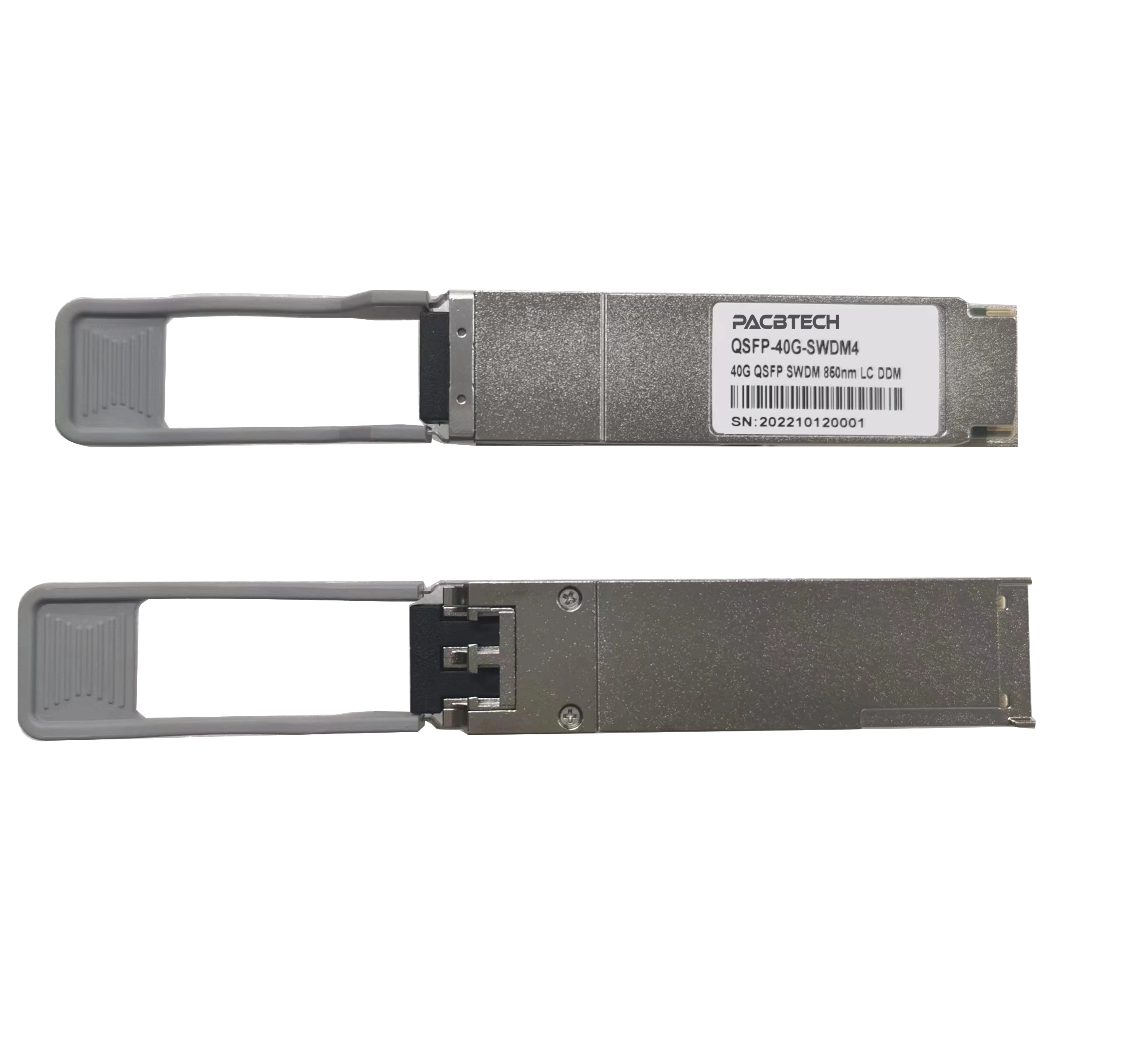


40G QSFP SWDM4 Optical Tranceiver
Multimode Duplex LC
Distance:
OM3-240Meters
OM4-350Meters
OM5-440Meters
The 40G QSFP+ SWDM4 transceiver modules are designed for use in 40G Ethernet links over duplex multimode fiber. Four channels/lanes in the 850-940nm region @ 10Gbps to transport the Ethernet signal. Digital diagnostics functions are available via an I2C interface, as specified by the QSFP+ MSA.
Applications
40G Ethernet over Duplex MMF
Feature
Compliant with QSFP+ MSA
Compliant with SWDM MSA
Compliant with SFF-8636
Compliant with IEEE 802.3ba
Hot-pluggable QSFP+ form factor
4x10Gb/s VCSEL-based SWDM transmitter
Supports 41.2Gbps aggregate bit rate
Power dissipation<3.5W
Maximum link length of 240m on OM3 MMF and 350m on OM4 MMF
Case temperature range of 0°C to 70°C
Duplex LC receptacles
XLPPI electrical interface
RoHS complian
1. Absolute Maximum Ratings
Parameter | Symbol | Min | Max | Units |
Storage Temp Range | Ts | -40 | +85 | ℃ |
Supply Voltage | Vcc | -0.5 | 3.6 | V |
Relative Humidity | RH | 15% | 85% |
2. Operating Conditions
Parameter | Symbol | Min | Max | Units |
Case Temp-Operating | Tcase | 0 | 70 | ℃ |
Supply Voltage | Vcc | 3.14 | 3.46 | V |
Power Consumption | P | 3.5 | W | |
Link Distance on OM3 Fiber | 2 | 240 | M | |
Link Distance on OM4 Fiber | 2 | 350 | M | |
Link Distance on OM5 Fiber | 2 | 440 | M |
3. Optical Characteristics
Transmitter Parameter | Lane | Min | Typical | Max | Unit | Note |
Signaling rate, each lane | 10.3125 , 9.953±100ppm | Gb/s | ||||
Lane Wavelength Range | Lane0 | 844 | 858 | nm | ||
Difference in launch power between any two lanes | 4.5 | dBm | ||||
RMS Spectral width @850nm @880nm,910nm,940nm | Lane0 Lane1,2,3 | 0.53 0.59 | nm | |||
Optical Modulation Amplitude (OMA), each lane | -5.5 | 3 | dBm | |||
Average Launch power per Lane | -7.5 | 3 | dBm | |||
Launch Power Tx OMA-TDP | Lane0 | -6.4 -6.0 -6.5 -7.0 | dBm | |||
Transmitter and Dispersion Eye Closure | Lane0 | 3.7 | dB | |||
Extinction Ratio | 2 | dB | ||||
Optical Return Loss Tolerance | 12 | dB | ||||
Average Launch Power per Lane @ TX Off State | -30 | dBm | ||||
Encircled Flux | >=86% at 19um <=30% at 4.5um | |||||
Transmitter eye mask definition {X1, X2, X3, Y1, Y2, Y3} | {0.23,0.34,0.43,0.27,0.35,0.4} | |||||
Receiver Parameter | Lane | Min | Typical | Max | Unit | Note |
Signaling rate, each lane | 10.3125 , 9.953±100ppm | Gb/s | ||||
Lane Wavelength Range | Lane0 | 844 | 858 | nm | ||
Lane1 | 874 | 888 | ||||
Lane2 | 904 | 918 | ||||
Lane3 | 934 | 948 | ||||
Damage threshold, each lane | 3.8 | dBm | ||||
Average Receive Power, each lane | -12.9 -12.5 -12.2 -11.9 | 2.4 | dBm | |||
Receiver Power, each lane (OMA) | 3 | dBm | ||||
Receiver sensitivity OMA, per lane | -9.1 | dB | ||||
Difference in receive power between any two lanes(OMA) | 5 | dB | ||||
RX_Los_Assert | -30 | dBm | ||||
RX_Los_De-ASSERT | -13 | dBm | ||||
RX_Los_Hysteresis | 0.5 | dBm | ||||
Return reflectance | -12 | dB | ||||
4. Digital Diagnostic Monitoring Specifications
Parameters | Unit | Specification |
Temperature Monitor | °C | ± 3 |
Voltage Monitor | V | ± 5 % |
I_bias Monitor | mA | ± 10 % |
Received Power (Rx) Monitor | dB | ± 3.0 |
Transmit Power (Tx) Monitor | dB | ± 3.0 |
5. Electrical Characteristics
Transmitter electrical input signal charactoristics(TP1) | Min | Typical | Max | Units | Conditions |
Single ended input voltage tolerance | -0.3 | 4 | V | Referred to TP1 signal common | |
AC common-mode input voltage tolerance | 15 | mV | RMS | ||
Differential input return loss | See 86A.4.1.1 | dB | 10MHz to 11.1GHz | ||
Diffrential to common-mode input return loss | 10 | dB | 10MHz to 11.1GHz | ||
J2 Jitter tolerance | 0.17 | UI | |||
J9 Jitter tolerance | 0.29 | UI | |||
Data Dependent Pulse Width Shrinkage(DDPWS) tolerance | 0.07 | UI | |||
Specification values | |||||
Eye mask coordinates: | 0.11,0.31 | UI | Hit Ratio=5E-5 | ||
Crosstalk calibration signal VMA | 850 | mV | While calibrating com-pliance signal | ||
Crosstalk calibration signal transition times, 20% to 80% | 34 | ps | |||
Receiver electrical output signal charactoristics(TP4) | Min | Typical | Max | Unit | |
Single ended output voltage tolerance range | -0.3 | 4 | V | Referred to signal common | |
AC common-mode output voltage (RMS) | 7.5 | mV | |||
Termination mismatch at 1MHz | 5 | % | |||
Differential output return loss | See 86A.4.2.1 | dB | 10MHz to 11.1 GHz | ||
Common-mode output return loss | See 86A.4.2.2 | dB | 10MHz to 11.1 GHz | ||
Output transition time,20% to 80% | 28 | ps | |||
J2 Jitter output | 0.42 | UI | |||
J9 Jitter output | 0.65 | UI | |||
Specification values | |||||
Eye mask coordinates: |
| UI | Hit ratio=5E-5 | ||
Crosstalk source VMA, each lane | 700 | mV | At TP1a | ||
Crosstalk source transition times,20% to 80% | 37 | PS | At TP1a | ||
Copyright © 2025 . Pacific Brands Technology Limited All rights reserved.